
Programming the MCU
The microcontroller part runs a short program that you write on its Code tab, in a small language made for pins. Name a pin in the code and it appears on the chip. The pins behave like real ones: an input can float, an output has a drive limit, and I²C needs pull-up resistors.
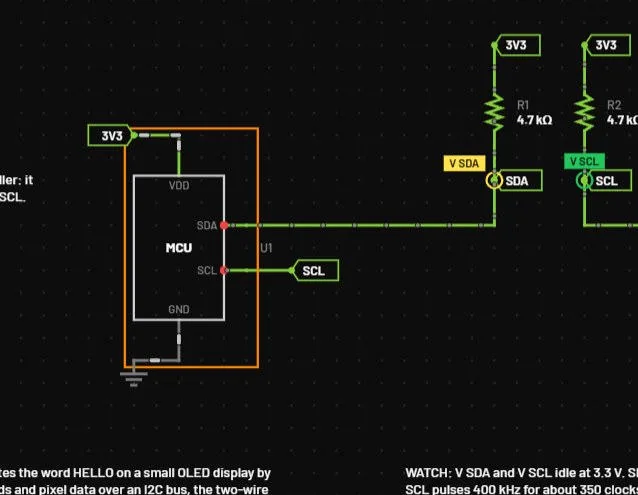
bus OLED i2c SDA SCL 400kHz: the chip has VDD, GND, SDA and SCL, and nothing else. R1 is one of the two pull-ups.41.1What the MCU part is
The part is mcu (designator U), placed from the library: type microcontroller in the search box and pick the tile MCU · Generic (family "Microcontrollers and processors"). It has VDD at the top and GND at the bottom. Every pin you declare in the code is added in the order you wrote it: inputs on the left, everything else on the right.
| You want | Do this |
|---|---|
| Your own pins and a program | Use the Generic variant (the default). Write the program on the Code tab. Pins come from the code. |
| A real package, such as ATmega328P, ATtiny85 or STM32F103C8 | Pick that variant. The pins are the package pins, and the names you declare must be pin names of the chip, for example pin PB5 out. |
The old script API (fn step(), pinmap) | A program that contains fn name( still runs as before, as for the control block (Programmable control blocks). Everything below is the new language. |
The program runs in the live simulation and in Simulate, on the same pins, in simulated time. Several MCUs in one circuit each run their own program. It runs from the top when the supply comes up, and stops when VDD falls below the brown-out level.
41.2Your first program: Blink
This program blinks an LED once a second and takes about five minutes to build. The LED pin of the chip toggles every 500 ms, and the LED lights in step.
- Press Ctrl+N for a new circuit. Press V, click once, then press G and click under it. Set the source to
3.3V and wire its two pins.You should seeA 3.3 V source with a ground. This is the supply. - Click the library search box, type
microcontroller, and click the tile MCU · Generic. Click the sheet to place it, then press Esc.You should seeA box named U1 with only VDD and GND. Wire VDD to the + of the source and GND to ground. - Select U1. In the inspector click the Code tab. Open the Template… list and pick Blink.You should seeThe code box holds
pin LED outand aloop. The chip now has a third pin, LED, on its right side. - Place a resistor (R,
330Ω) and an LED (typeLEDin the library search and click the red LED), and wire LED pin → R1 → LED anode → LED cathode → ground. Press P and click the wire at the LED pin.You should seeA probe tag V LED pin on the wire. - Press Ctrl+R if the simulation is paused.You should seeThe pin goes between 0 V and 3.3 V every 500 ms on the scope, the LED lights and goes dark, and the current through it’s about 4 mA.
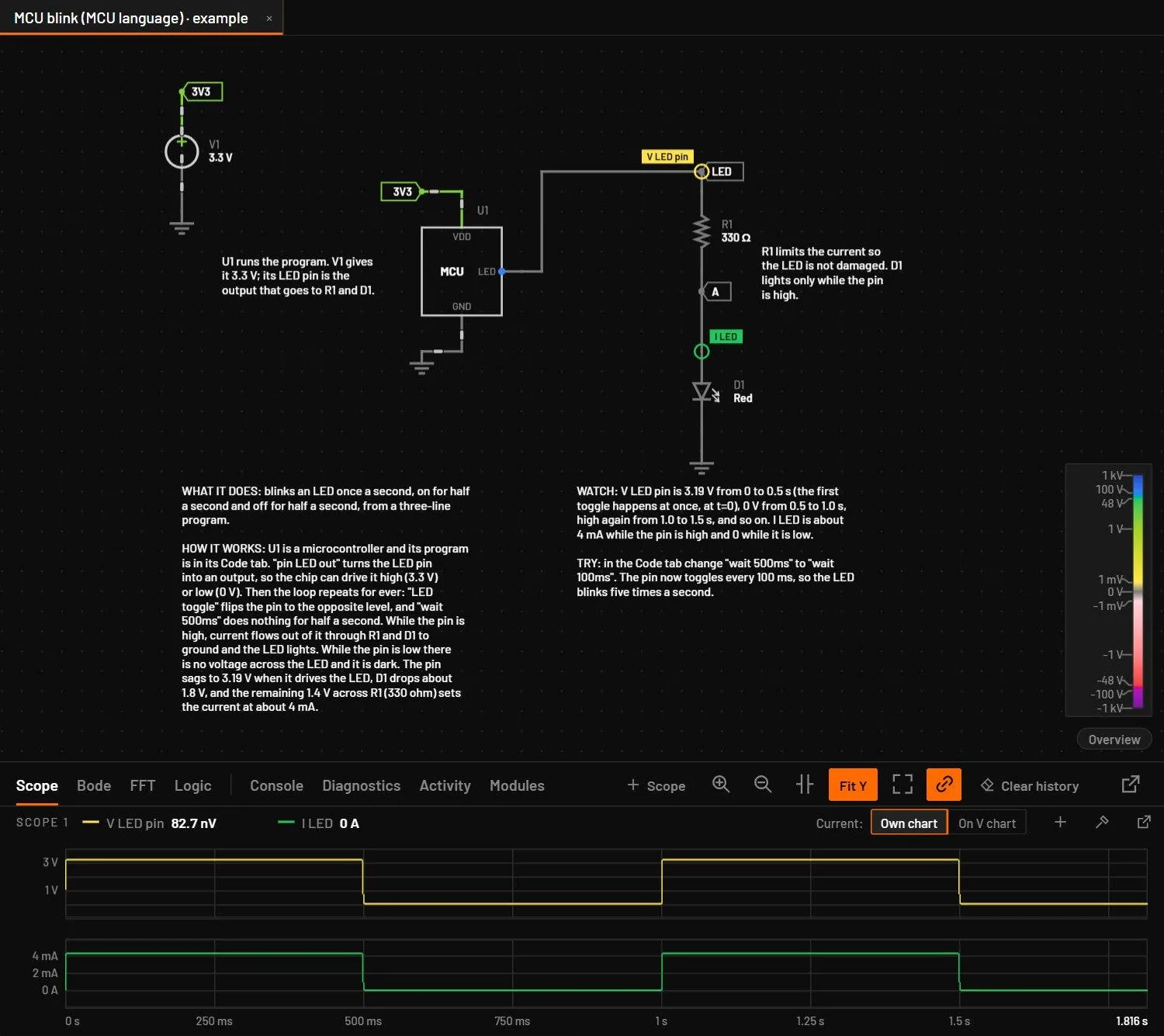
pin LED out and that the Code tab shows No script errors.
If you seethe pin toggles but the LED stays dark, the LED is wired the wrong way round, or its current path is open. Probe the wire between R1 and the LED.
The Code tab is the whole editor:
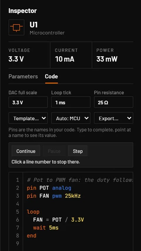
| Part of the tab | What it does |
|---|---|
| DAC full scale, Loop tick, Pin resistance | Quick fields for vdd, tick and rout (Parameters). |
| Template… | Replaces the code with a ready program (Templates and examples). One undo step. |
| The code box | Colours for keywords, pin kinds and numbers. Tab inserts two spaces. A line with an error is marked red in the gutter. |
| The status line | No script errors, or Line N: and what to write instead. Circuit warnings (W_MCU_PIN, W_MCU_BUS) show here with their fix too. |
| Syntax | A fold-out list of every statement with a one-line meaning. |
The code applies when you leave the editor or press Ctrl+S in it. Editing the code redraws the chip. Wires stay on every pin that keeps its name.
41.3Declarations: pin and bus
Declarations come first. Each adds pins to the chip, named as you write them. Names are case-sensitive, and a name can be used once.
| Line | Adds | Options |
|---|---|---|
pin NAME out | Digital output | opendrain: pulls low only. high: starts high. |
pin NAME in | Digital input | pullup or pulldown: an internal 40 kΩ. |
pin NAME analog | ADC input, reads volts | bits N (default 12). |
pin NAME dac | Analog output, volts | bits N. |
pin NAME pwm FREQ | PWM output, value is the duty 0 to 1 | FREQ such as 25kHz. |
pin NAME complement PWMPIN [dead TIME] | Complementary PWM output of a pwm pin declared above it | dead 200ns: dead time before each output turns on. Set the duty on PWMPIN, not on NAME. |
bus NAME uart TX RX [baud] | Two pins, TX and RX | Baud, default 9600. |
bus NAME i2c SDA SCL [rate] | Two open-drain pins, master | Rate such as 400kHz (default 100 kHz). |
bus NAME spi SCK MOSI MISO CS [rate] | Four pins, master, mode 0 | Rate such as 1MHz (default 1 MHz). |
bus NAME can TX RX [rate] | Two pins, standard frames | Rate such as 500k (default 500 kbit/s). |
Pins on the left of the chip are the inputs (in, analog, UART RX, SPI MISO, CAN RX). The names after a bus (TX, SDA) are the pin names. The first word (U, OLED) names the bus in the program: send OLED …. A pin cannot also be a supply pin: VDD and GND are reserved.
41.4Blocks: loop, every and when
Lines outside a block run once at the start, in order. A block is closed with end. Several blocks run side by side, each with its own place in its code, so a wait in one never stops another.
| Block | Runs | Example |
|---|---|---|
loop … end | Over and over. A pass that waits for no time lasts one tick (1 ms), so a loop without wait never hangs the simulation. | loop / LED toggle / wait 1s / end |
every TIME … end | Periodically, from the start, with no drift. every 1kHz works too. | every 100ms |
when PIN rises … end | When the pin goes high (falls: low, changes: either). The edge is found at its exact instant. | when BTN falls |
when BUS gets … end | When a UART byte or a CAN frame arrives. Read it with BUS.byte, BUS.id. | when U gets |
everyandwhenblocks run beforeloopat the same instant, like interrupts.- An
everyorwhenblock that is still running when it’s due again is skipped. wait TIMEpauses only its own block. The time counts from when the block woke up, so a loop ofwait 10msdoesn’t drift.- A
sendorreadholds its own block until the transfer is done. While one block uses a bus, another block’s transfer on that bus queues.
41.5Statements
| Statement | What it does | Example |
|---|---|---|
NAME on / off / toggle | Set a digital output (high and low work too). | LED toggle |
NAME = EXPR | Write a pin (a level, a PWM duty 0 to 1, or volts on a DAC), or set a variable. | FAN = POT / 3.3V |
wait TIME | Pause this block. The unit is required. | wait 10ms |
if C / else if C / else / end | Condition. | if BTN is low |
while C … end | Repeat while the condition holds. | while BTN is high |
repeat N … end | Repeat N times. | repeat 8 |
print ITEMS | One line in the Console: texts and values, separated by spaces. | print "v =" POT |
send BUS ITEMS [into VAR] | UART: text and bytes. I²C: the 7-bit address, then bytes. SPI: bytes (into receives the bytes read). CAN: an id, then up to 8 bytes. | send OLED 0x3C 0x00 0xAF |
read BUS … into VAR | UART: the next byte (waits for it). I²C: ADDR COUNT. SPI: COUNT. | read T 0x48 2 into raw |
font "TEXT" | Inside a send: the 5 × 7 font column bytes of the text, for a display. | send OLED 0x3C 0x40 font "HI" |
Variables are global. Each one must be set somewhere in the program, or the code is refused with y has no value: set it first. Until that line runs, the variable reads 0. Write a negative number in brackets inside print and send: (-1).
41.6Expressions, units and functions
| Item | Forms | Notes |
|---|---|---|
| Numbers with units | 10ms 100us 2s 25kHz 1MHz 3.3V 4k7 50% | A time needs its unit: wait 10 is an error. 50% is 0.5. |
| Hex and binary | 0x3C 0b1010 | Bytes sent are round(value) & 0xFF. |
| Arithmetic | + - * / % | |
| Bits (whole numbers) | & | << >> | |
| Comparison | < > <= >= == != | True is 1, false is 0. |
| Logic | and or not, X is high, X is low | true, false, high and low are 1 or 0. |
| Time | time | Seconds since the start. |
| Functions | min(a, b) max(a, b) abs(x) clamp(x, lo, hi) round(x) floor(x) map(x, a, b, c, d) | map(POT, 0, 3.3, 0, 255) turns volts into a byte. |
| Reading a pin | the pin’s name | A digital input reads 0 or 1, an analog input volts, an output its level, a PWM pin its duty, a DAC pin its volts. |
| Fields | .counts .byte .byte(k) .len .id .ack | POT.counts is the raw ADC code. OLED.ack is 1 if the last I²C address was answered. CAN.byte(0) is the first data byte. |
| Comments | # or // | To the end of the line. |
41.7Errors in the code
A mistake in the program is an E_SCRIPT error. The message names the line and column and says what to write. It shows under the code and in the Diagnostics tab, and the line is marked red. The program doesn’t run until it’s fixed.
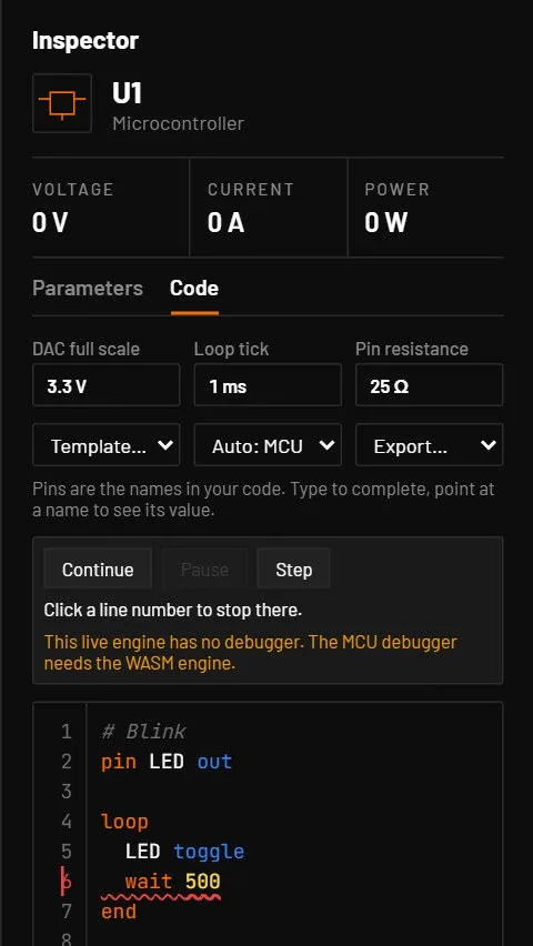
wait 500 has no unit: line 6 is marked and the message says what to write.| Message | Fix |
|---|---|
| "FAN is a pwm pin; write FAN = 0.5 for 50 % duty" | Write a duty from 0 to 1 (or 50%), not on. |
| "wait 10 needs a unit: write wait 10ms or wait 10s" | Add the unit. |
| "y has no value: set it first (e.g. y = 0) or declare it as a pin" | Assign the variable before the first line that reads it. |
| "this never runs: the loop on line 2 repeats forever …" | Lines after a loop in the same block can never run. Put them above it, or in an every or when block. |
| … is a supply pin | Do not declare VDD or GND. Use other names for I/O pins. |
| "… = 2 is above 1; a pwm duty goes from 0 to 1" (a warning) | Scale the duty to 0 to 1. |
41.8GPIO: outputs and inputs
pin LED out
pin BTN in pullup
pin SDA_X out opendrain
pin CS out high
| Part | What happens electrically |
|---|---|
| Output | Driven from the chip’s own VDD and GND pins through rout (25 Ω), with 10 ns edges. An output isn’t a power source: with the supply unwired it cannot drive anything. |
| Open-drain output | Pulls low only. It needs a pull-up to go high. |
| Drive limit | More than imax (25 mA) for 10 µs warns W_MCU_PIN. If the pin sits at the opposite level the message says it’s shorted or fights another output. |
| Input | Low below 0.3 VDD, high above 0.7 VDD, with hysteresis, measured against the actual supply. |
pullup, pulldown | An internal 40 kΩ resistor to VDD or GND. A push button to ground needs nothing else. |
| A floating input | A pin with no pull and nothing connected rests at half the supply, reads random bits, and warns W_MCU_PIN after 1 ms. |
| Edge events | when BTN falls runs at the exact instant the input crosses its threshold, not on the next tick. |
- Open Digital control and the example MCU button to LED with the internal pull-up.
- Click the switch SW1 while it runs.
- Select U1, open the Code tab and delete the word
pullup.
You should seeThe LED follows the switch within 10 ms. After you delete pullup, the pin BTN floats and the warning W_MCU_PIN appears in about a millisecond.
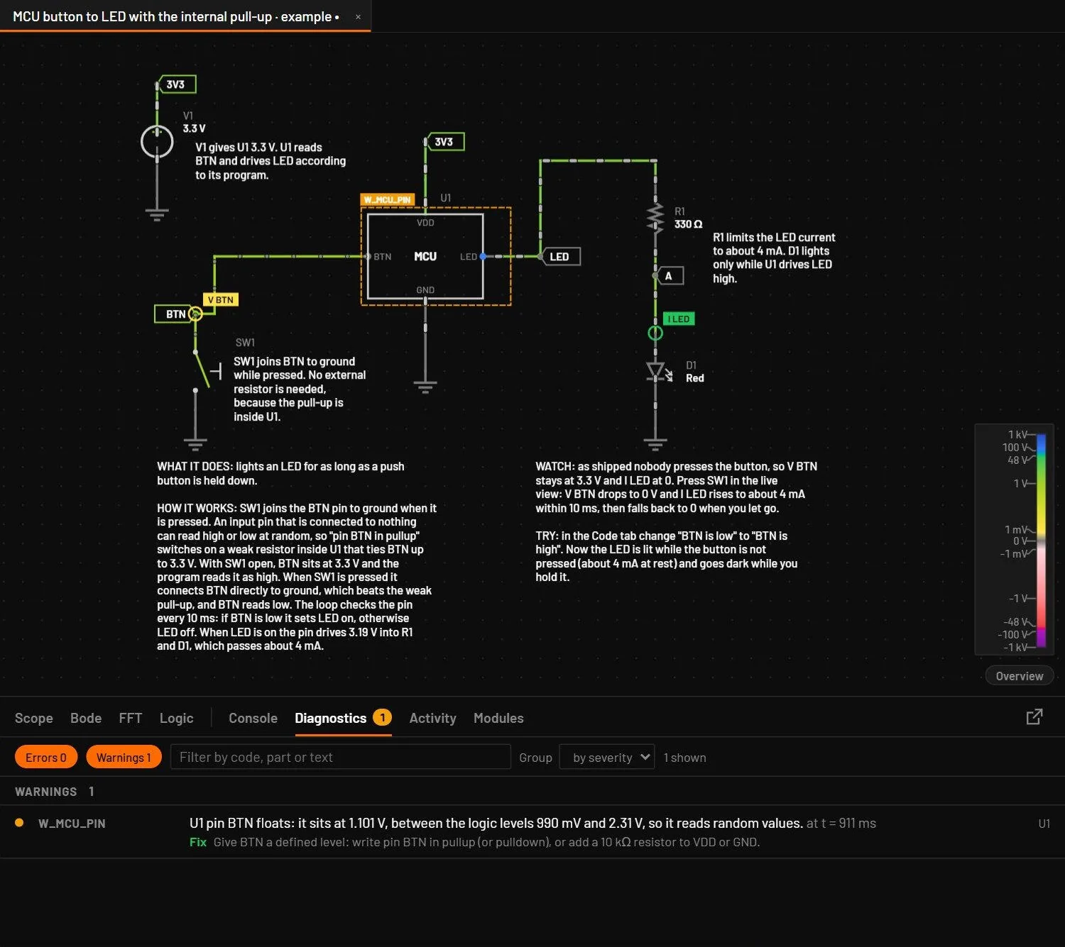
pullup the input BTN floats. The warning names the pin, the level it sits at and the fix.41.9ADC and DAC
pin POT analog bits 10
pin OUT dac

every 100ms
  print "pot" POT "V," POT.counts "counts"
end

OUT = 1.2V
- ADC: the pin voltage is measured at the instant it’s read and quantised against the actual supply, with
bitsbits (default 12).POTreads volts,POT.countsthe code. If VDD sags, the reading changes, as on a real chip. - DAC:
OUT = 1.2Vsets the coderound(v / vdd · (2bits − 1)). The pin drives that fraction of the actual supply through rdac (100 Ω). Set the full scale with vdd in the quick fields.
41.10PWM
pin FAN pwm 25kHz

loop
  FAN = POT / 3.3V
  wait 5ms
end
The edges are exact, not sampled on a tick. A new duty takes effect at the next period, as with a timer preload register. The pin reads back its duty, and the live values show FAN_duty. A duty above 1 is clamped and warns.
Complementary outputs with dead time
A half bridge needs two outputs that are never on together. Declare the second pin as the complement of the first, with a dead time:
pin HI pwm 20kHz
pin LO complement HI dead 200ns

HI = 0.3
LO follows the period and the duty of HI, including the rule that a new duty starts at the next period. HI goes high one dead time after the period starts and low at duty · T. LO goes high one dead time after HI falls and low at the end of the period. They are never high together, and the edges are exact. At duty 0 and duty 1 the pins hold steady levels, with no dead-time notches, as a timer does at CCR = 0 and CCR = ARR. A pwm pin has at most one complement, and the complement is drawn on the right of the chip like any output.
- Write the duty on the main pin.
LO = 0.5is an error: "LO is a complementary pwm pin; it follows its pwm pin. Set the duty on that pin". - The main pin must be a pwm pin declared above the complement, and
deadneeds a time (dead 200ns).
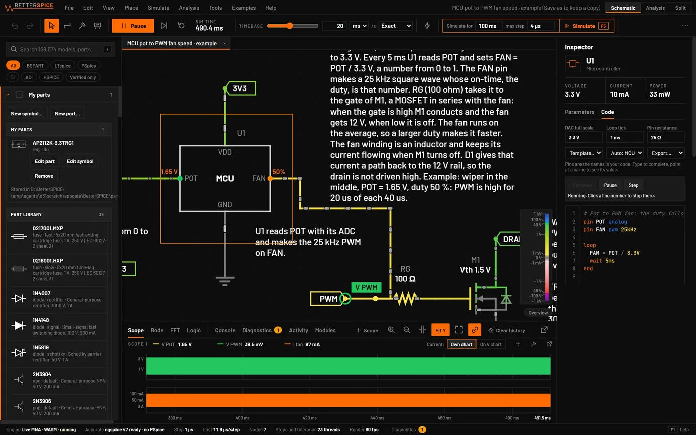
- Open Digital control and MCU pot to PWM fan speed.
- Click the potentiometer RV1 and change its wiper with the slider.
You should seeThe duty and the fan current follow the pot. M1 switches the 12 V fan, and D1 catches the motor current when M1 turns off.
41.11UART
bus U uart TX RX 9600

loop
  send U "hi" 10
  wait 1s
end

when U gets
  print "got" U.byte
end
- Each byte is sent as 8N1, bit by bit at the baud rate. The TX line idles high.
- The receiver samples in the middle of each bit, from the start edge it finds. A low stop bit is a framing error:
W_MCU_BUSsays the baud rates probably differ. - Wire TX of one chip to RX of the other. A floating RX warns, because an idle line must be high.
send U "text" 10 0x41sends text and bytes.read U into xwaits for the next byte.- To talk to the PC, wire TX and RX crossed to a USB-UART bridge (
chip, variantusb_uart) at the same baud rate. What the MCU sends shows in the Console as lines, and text typed in the Console input bar arrives inwhen U gets(Chips and displays).
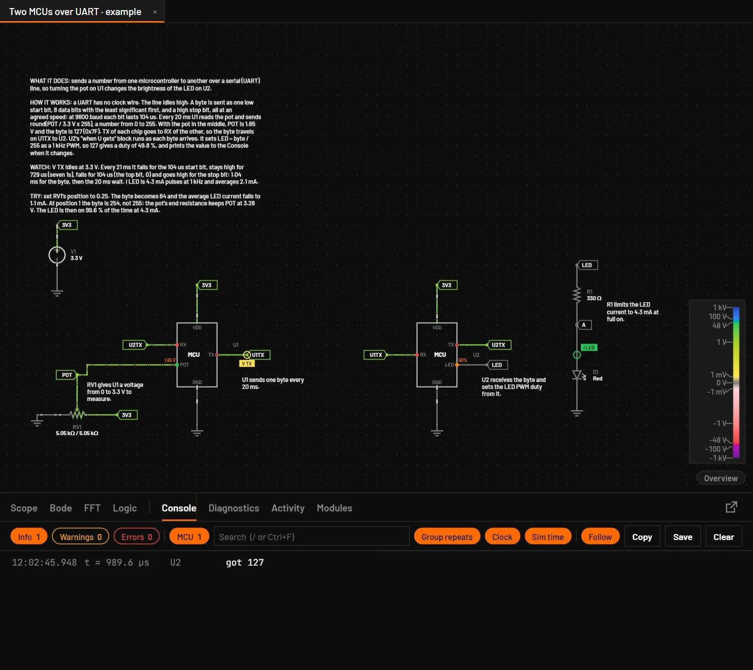
- Open Digital control and Two MCUs over UART.
- Open the Console (Alt+5) and turn the pot.
You should seeU2 prints got 127, got 140 and so on as the byte changes, and its LED brightness follows.
41.12I²C
bus OLED i2c SDA SCL 400kHz

send OLED 0x3C 0x00 0xAF
if OLED.ack == 0
  print "no answer: check the address and the pull-ups"
end
read OLED 0x48 2 into t
| Part | What happens electrically |
|---|---|
| Lines | SDA and SCL are open-drain. They go high only through pull-up resistors, so the circuit needs 2.2 kΩ to 10 kΩ from each to VDD. |
| Timing | Quarter-bit steps at the chosen rate (100 kHz or 400 kHz). Both lines are checked to rise when released, at START and at every SCL high. |
| No pull-up | The transfer fails, OLED.ack is 0, and W_MCU_BUS says "add a pull-up resistor (2.2 kΩ to 10 kΩ)". |
| A line held low | A target holding it, a short, or a pull-up far too weak for the bus. The warning says to use a stronger pull-up. |
| Wrong address | No target answers (NACK). The transfer stops, .ack is 0, and W_MCU_BUS warns. |
| Targets | The SSD1306 and the digital potentiometer (I²C) answer by pulling SDA low. So do the EEPROM and the RTC chips (Memory, flash and RTC chips). |
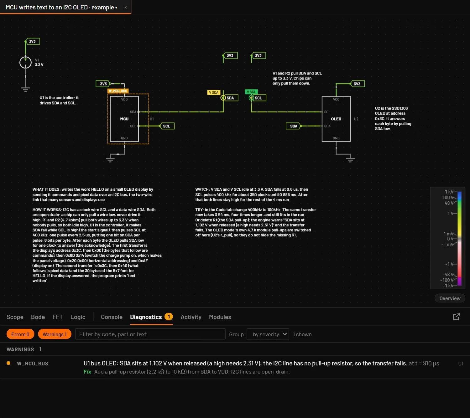
- Open Digital control and MCU writes text to an I2C OLED.
- Select U2, the display, and look at its symbol.
- Delete R1 and R2.
You should seeThe display shows HELLO. After the pull-ups go, the Console prints no answer from the OLED and Diagnostics shows W_MCU_BUS.
41.13SPI
bus DAC spi SCK MOSI MISO CS 1MHz
code = 0

loop
  send DAC 0x00 code
  code = (code + 1) % 129
  wait 1ms
end
- Mode 0, chip select active low. CS goes low, MOSI changes while SCK is low, MISO is read on the rising edge, and CS goes high after the last byte.
send S 0x12 0x34 into rtransfers two bytes and puts what came back inr.read S 2 into rclocks out zeros and reads two.- While the MCU is in reset, a CS with no pull-up floats, and a target could be selected at power-up.
W_MCU_BUSsays "add a 10 kΩ pull-up from CS to VDD". - Use
pin CS out highinstead of a bus CS when you need several targets on one clock.
41.14CAN
bus CAN can TX RX 500k
pin BTN in pullup

loop
  send CAN 0x100 (BTN is low) * 255
  wait 10ms
end

when CAN gets
  if CAN.id == 0x100
    print "button" CAN.byte(0)
  end
end
- Standard 11-bit data frames, sent bit by bit with stuffing and a CRC. Receivers destuff, check the CRC and pull the ACK slot dominant.
- A node waits for 11 recessive bits before it sends or accepts a frame.
- Use a CAN transceiver (the
canpart: CANH, CANL) and a 120 Ω termination at each end of the bus. TX and RX can also be cross-wired directly for a logic-level bus. - A frame nobody acknowledges sets
CAN.ackto 0 and warnsW_MCU_BUS: connect a second node with awhen CAN getsblock, at the same bit rate.
- Open Digital control and Two MCUs on a CAN bus.
- Click SW1 while it runs.
You should seeU2 lights its LED while SW1 is pressed, and prints every 50th frame. RT1 and RT2 are the terminations.
41.15Memory, flash and RTC chips
Five variants of the chip part answer the I²C and SPI masters, so a program can read and write them (Chips and displays).
| Chip variant | Bus and address | What it does |
|---|---|---|
eeprom (24C02) | I²C, 0x50 plus A2 A1 A0 | 256 bytes, 8-byte page write, a 5 ms write cycle during which it doesn’t answer its address (poll with .ack), sequential read, WP high ignores writes. |
spi_flash (W25Q) | SPI mode 0, nCS | JEDEC id 0x9F (EF 40 15), read 0x03, write enable 0x06, status 0x05, page program 0x02 (only 1 to 0), sector erase 0x20 (45 ms). |
rtc (DS1307) | I²C, 0x68 | BCD seconds, minutes, hours, day, date, month and year registers that count simulated time. The clock starts when the seconds register is written. |
i2c_dev (any I²C sensor) | I²C, addr (0x48), +1 with ADDR high | Your register map (regs, ro) and a live reading you drag. send D 0x48 REG BYTES writes from REG. send D 0x48 REG then read D 0x48 N into x reads N registers from REG. Other addresses aren’t acknowledged. |
spi_dev (any SPI peripheral) | SPI mode 0 (cpol, cpha), CS | The same register map. send D REG BYTES writes from REG, and send D 0x80+REG 0 0 reads, the data in D.byte(1) on. |
bus RTC i2c SDA SCL 100kHz
send RTC 0x68 0 0x00 0x30 0x12   # register 0, then 00 s, 30 min, 12 h
loop
  send RTC 0x68 0
  read RTC 0x68 3 into t
  s = (RTC.byte(0) >> 4) * 10 + (RTC.byte(0) & 15)
  print "seconds" s
  wait 1s
end
The fourth variant, usb_uart, is a USB-to-UART bridge whose USB side is the Console. It’s the way to talk to the PC from a program (Chips and displays).
41.16Reset, brown-out and supply current
- While the circuit finds its DC operating point, and whenever VDD is below vbor (1.8 V), the pins are released and the program is stopped. It starts again from the top when the supply returns.
- The chip draws idd (10 mA) from VDD to GND, plus every pin’s drive current. The live values show
idd,vddand whether the program is running.
41.17Warnings you may see
The language check finds mistakes in the program. These warnings find mistakes in the circuit around it. They appear in the Diagnostics tab (Alt+6) and under the code.
| Code and message | Cause | Fix |
|---|---|---|
W_MCU_PIN "pin BTN floats: it sits at 1.1 V, between the logic levels … so it reads random values" | An input or UART RX with nothing driving it, for 1 ms. | Write pin BTN in pullup (or pulldown), or add a 10 kΩ resistor to VDD or GND. For RX, wire it to the other side’s TX. |
W_MCU_PIN "pin LED sources 40 mA (an MCU pin is rated about 25 mA)" | An output loaded more than imax for 10 µs. | Add a series resistor (about 330 Ω for an LED) or drive the load through a transistor. |
W_MCU_PIN "pin X drives high but sits at 0.2 V … shorted to ground or fights another output" | Two outputs tied together, or an output wired to a rail. | Never join two outputs. Use an open-drain output with a pull-up for a shared line. |
W_MCU_BUS "SDA sits at 0.0 V when released … has no pull-up resistor" | An I²C line with no pull-up. | Add 2.2 kΩ to 10 kΩ from SDA and SCL to VDD. |
W_MCU_BUS "no target answered (NACK) on line 7" | Wrong address, target not powered, or not wired. | Check the 7-bit address, the target’s supply and the wiring. |
W_MCU_BUS framing error | The baud rates of the two UARTs differ. | Use the same rate in both bus … uart lines. |
W_UART "framing error on RXD (the stop bit is low) …" | A USB-UART bridge received a byte at another baud rate than its own. | Set the bridge’s baud to the MCU’s rate (Chips and displays). |
W_MCU_BUS "chip select CS floats while the MCU is in reset" | An SPI target could be selected at power-up. | Add a 10 kΩ pull-up from CS to VDD. |
W_MCU_BUS "nobody acknowledged the CAN frame" | No other node, or a different bit rate. | Add a second node with when CAN gets and 120 Ω terminations. |
E_SCRIPT U1 line 3 col 3: … | A mistake in the program. | Fix the line the message names. |
41.18Arduino style, pin names and board names
The code can look like Arduino code. Braces, setup and loop, pinMode, digitalWrite(PIN, HIGH), digitalRead, analogRead, analogWrite, delay, millis, Serial.println, fn with return, every(50us) { } and on(BTN, FALLING, debounce: 20ms) { } all work. The older line statements (LED on, wait 10ms, loop ... end) still work in the same program, and old programs run exactly as before. The Arduino style is translated onto the same runtime, so a program in either style gives the same waveforms, and an error still names the line and column you wrote.
pin BTN in pullup
pin FAN pwm 25kHz
let level = 0

on(BTN, FALLING, debounce: 20ms) {
  level = (level + 1) % 4
  duty(FAN, level / 3)
}
A name becomes a pin of the chip as soon as the code uses it, and its role is taken from its use or from pinMode. Two uses that disagree are an error that names both lines. You can also name a chip pin yourself: pin VOUT = PA0 analog 12bit makes the chip pin PA0 the pin VOUT in the code. The symbol keeps the chip's pin name and draws your name in small type beside the lead. On the ATmega328P, ATtiny85 and STM32F103 variants the board names also work, such as D13, A0 and LED_BUILTIN. A name that is not a pin of the chip is an error with a Did you mean. The Language box on the Code tab (Auto, MCU language, Rhai) fixes the language when Auto guesses wrong. The MCU language runs on the WASM engine, which is the default, and from 0.8.0 on the JavaScript fallback too, with the same pins, timing, buses, messages, debugger and displays.
41.19Editor help
- Completion: typing offers the pins of the part, the keywords and the Arduino names. It knows the context:
analogRead(offers analog pins,pinMode(P,offers the modes,on(P,the edges. Tab or Enter takes one, Esc closes the list and Ctrl+Space opens it. - Hover: pointing at a pin name shows its value now, for example
VOUT (PA0): analog input, 12bit. 1.20 V, 1495 counts. Pointing at a word of the language shows its form. Pointing at an error shows its sentence. - Errors: a wavy underline from the error column over the token, the plain sentence below it with a click to jump to the line, and Did you mean from a distance check over pins, variables, keywords and functions.
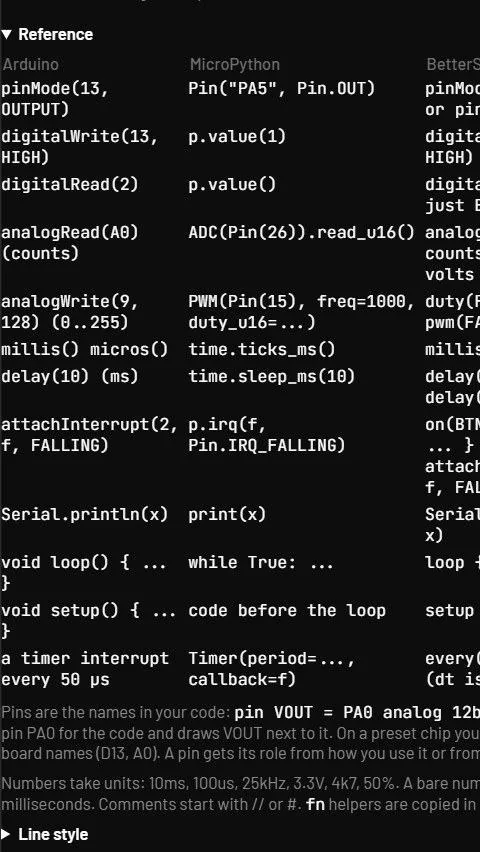
- Reference card: below the editor, a three-column cheat sheet (Arduino, MicroPython, BetterSPICE). The line style is folded below it.
- Enter keeps the indent and adds one after an opening brace.
41.20Pin colours and the pin map
While the simulation runs, a dot where each lead meets the symbol shows what the pin is doing.
| Colour | Meaning |
|---|---|
| Red | High. |
| Blue | Low. |
| Grey | Floating. |
| Orange | PWM, with its duty in percent. |
| Green | Analog, with its volts. |
The Pin map under the editor lists each pin with its chip pin, its role and its value now. Its Scope button adds a probe on the pin and its Logic button adds a logic analyzer channel at half the supply. Clicking a pin name jumps to its line in the code.
41.21Debugging: breakpoints, Step and Variables
Click a line number in the Code tab gutter to set a breakpoint, shown as an orange dot. A hollow dot marks a line that holds no statement, so it never stops there. Breakpoints belong to the part, move with their lines when you add or remove lines above them, and can be undone.
When the program reaches a breakpoint, the simulation stops at that instant, the MCU is selected, its Code tab opens, the line is highlighted, the bar says Paused at line 8, in when U gets, at 127.2 ms and the Console gets the same line. Step runs the next statement of this MCU. Across a wait the circuit runs as fast as it can until the program gets there, and after 4 seconds without a statement it stops and says the program is waiting for a time, a pin or a byte. Continue runs to the next breakpoint and then plays the live view. Pause stops at the next statement this MCU runs.
The Variables panel under the editor lists variables (the ones changed since the previous stop in orange), pins with their role, level, duty or ADC volts, buses with the last data and their state, and blocks (main, every, when) with the current line. It updates while paused and four times a second while running.
With several MCUs, each has its own breakpoints. When U2 holds the circuit, U1's bar says U2 paused at line 8 with a Show U2 link, and Continue or Step lets the held MCU carry on first. Stopping does not change the waveform: the rest of the instant runs after you resume, with no shift in time.
41.22Export to Arduino or STM32
The Export box in the Code tab saves a program in the Arduino style as an Arduino sketch (.ino) or an STM32 HAL file (main_app.c) with the same pin names. It is a starting point, not a finished firmware. Board pin numbers the chip does not give, the PWM frequency, the ADC and the timers are marked TODO where the chip needs a choice. A program in the line style is refused with a sentence that says so. The output has been read by eye and has not been compiled.
41.23Templates and examples
The Template… list on the Code tab fills the code box with a ready program. Wire the pins as the first comment line says.
| Template | What it does |
|---|---|
| Blink | Toggles an LED every 500 ms. |
| Button to LED | A push button to ground on BTN with the internal pull-up lights an LED. |
| Pot to PWM fan | The ADC reading of a pot sets a 25 kHz PWM duty. |
| Read a sensor and print it | Prints an analog sensor in volts and counts every 100 ms. |
| I2C OLED text | Starts an SSD1306 at 0x3C and writes HELLO. Needs the pull-ups. |
| SPI DAC sweep | Sweeps an SPI digital potentiometer wired as a DAC. |
| Two MCUs on UART | The sender. The receiver is in the comments, to paste into the second MCU. |
| Two MCUs on CAN | Node A sends the button state. Node B’s code is in the comments. |
Seven circuits in Examples › Digital control run these programs with the parts around them:
| Example | Shows |
|---|---|
| MCU blink | The smallest program. R1 limits the LED current. |
| MCU button to LED | A switch to ground with the internal pull-up. Delete pullup to see the floating warning. |
| MCU pot to PWM fan | ADC to 25 kHz PWM to a logic-level MOSFET and a 12 V fan with a flyback diode. |
| Two MCUs over UART | U1 sends its pot as a byte at 9600 baud. U2 sets an LED brightness and prints the value. |
| MCU writes text to an I2C OLED | The SSD1306 start-up and the text HELLO. R1 and R2 are the pull-ups. |
| Two MCUs on a CAN bus | Two MCUs through 3V3 transceivers, terminations, a button and an LED, frames acknowledged. |
| MCU reads an I2C real-time clock | Starts a DS1307-style RTC at 12:30:00 and prints the time every second. |
41.24Parameters
The part’s own settings, set in the inspector’s Parameters (the first three also on the Code tab), or in All parameters.
| Parameter | Key | Unit | Default | Range | Value comes from | What it does |
|---|---|---|---|---|---|---|
| DAC full scale (supply) | vdd | V | 3.3 | > 0 | Default, Code tab, part file | The supply that the logic levels, the ADC and the DAC are measured against. It’s the DAC full scale. |
| Loop tick | tick | s | 1 ms | > 0 | Default, Code tab, part file | How long a loop pass that waits for nothing lasts. |
| Pin resistance | rout | Ω | 25 | > 0 | Default, Code tab, part file | Output resistance of a push-pull pin. |
| Edge time | tr | s | 10 ns | ≥ 0 | Default, file | Output rise and fall time. |
| Pull resistance | r_pull | Ω | 40 kΩ | > 0 | Default, file | The internal pull-up or pull-down. |
| DAC output resistance | rdac | Ω | 100 | > 0 | Default, file | |
| Pin current warning | imax | A | 25 mA | > 0 | Default, file | Above this for 10 µs: W_MCU_PIN. |
| Brown-out voltage | vbor | V | 1.8 | > 0 | Default, file | Below it the program stops. |
| Supply current | idd | A | 10 mA | ≥ 0 | Default, file | Drawn from VDD to GND. |
| Program | code | text | empty | Code tab | The program, in the MCU language. |
Key: the name in the circuit file, in a parameter step (R1.r) and for AI agents. Range: a value outside it is refused with E_PARAM. Value comes from: where you can set it. The All parameters tab and agents can set every parameter.
41.25What is not emulated
Real microcontrollers have these. The model does not:
| Not emulated | Instead |
|---|---|
| Watchdog, sleep modes, DMA | Use every and wait. |
| The RTC calendar inside the MCU | Use an RTC chip on I²C. |
| Input capture, quadrature encoder mode | Use when PIN changes and count in a variable. |
| ADC triggered by PWM | Sample in an every block. |
| USB, Ethernet | Not available. |
| I²C and SPI target (slave) mode | The MCU is always the master. |
| CAN arbitration between senders that start together, remote and extended frames | Standard data frames only. |
| UART parity and 2 stop bits, SPI modes 1 to 3, I²C clock stretching | Fixed at 8N1 and mode 0. |