
Draw and edit
10.1Place, rotate and wire parts
Put parts on the sheet, turn them the right way and connect them.
Before you startAn open circuit. Ctrl+N starts a new one.
- Press the part's key, for example R for a resistor, or click its tile in the library.You should seeThe part follows the pointer.
- Press the same key again, or Space, to rotate it 90°. Ctrl+E mirrors it. Another part's key switches to that part.
- Click to drop it. Click again to drop another of the same part.
- Press Esc once to stop placing.
- Move the pointer onto a pin until it becomes a crosshair, drag to another pin and release.You should seeA wire joins the two pins. Each click of the Wire tool (W) places a corner instead.
ResultThe parts are connected and the live simulation runs them at once: wires take colour as soon as a loop closes.
| If you see | Do this |
|---|---|
| A second copy of the part when you meant to stop | Press Esc after the last drop, or Ctrl+Z to remove the extra one. |
| A wire end in mid-air | It missed the pin. Drag the end onto the pin: the pointer is a crosshair when it's on one. |
| Two wires cross but don't connect | Wires connect only at ends and pins. End one wire on the other: a junction dot appears. |
See alsoPlacing parts (every place key), Wires, Keyboard shortcuts by task.
10.2Name nets and use ground and power flags
Give nets names, so readings and probes say OUT and VCC, and join nets without drawing wires.
- Press N (net label) and click a wire.
- Type the name, for example
OUT, and press Enter. Names can't contain spaces: use an underscore. - For a supply, press Shift+G (power flag), click the wire and type
VCC. Every flag and label named VCC is one net. - Press G for ground: the 0 V reference, net
0. Every circuit needs one.
ResultHolding the pointer over a wire shows its name and voltage. Probes on it are named after it, like V OUT.
| If you see | Do this |
|---|---|
| "Type a name or press Esc." | An empty name is refused. Type one, or press Esc. |
| Two labels with the same name didn't join | Net labels join only on the same sheet. Use a global label (Shift+N) across sheets. |
See alsoLabels, flags and ground, Nets and ground.
10.3Keep sides isolated with their own grounds
Draw circuits whose sides don't share the main ground, such as the secondary of a transformer or the output of an optocoupler, and tie them together only through the isolating part.
Before you startA circuit with a main ground (G).
- Press G, then Tab until the ghost under the pointer is named
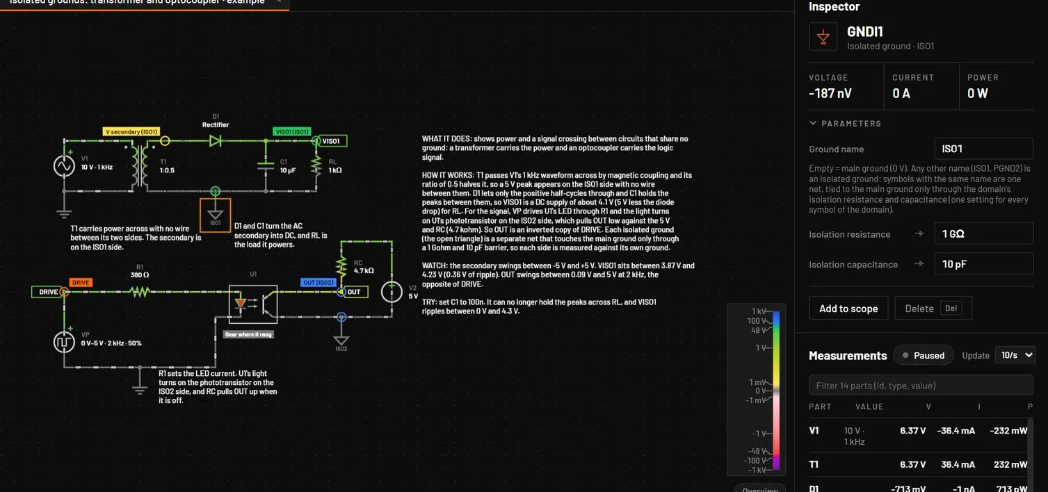
ISO1. Or open Sources in the library and take Isolated ground (the open triangle). Click it onto the 0 V wire of the isolated side.You should seeA message names the domain, for example Isolated ground ISO1 (new domain), and the name is under the triangle. - Place more grounds of the same name on that side as needed. Grounds with the same name are one net, like labels.
- For another isolated side, press Tab again while placing, until the name is a new one such as
ISO2. (Start a new ground domain has the other ways.) - Join the sides only through the isolating part: a transformer (Devices: passives), an optocoupler or a digital isolator.
- To read a voltage on an isolated side, press P and click its net. The probe is against that side’s own ground and says so, for example
V OUT (ISO2). Shift+click reads against the main ground instead and is namedV OUT (vs GND). - To change the isolation, select any ground of the side and edit Isolation resistance or Isolation capacitance in the inspector.You should seeEvery ground of that domain follows, in one undo step. The main ground has no isolation fields, only its name.
ResultEach isolated side is its own net family, tied to the main ground only through its isolation barrier: Isolation resistance (1 GΩ) in parallel with Isolation capacitance (10 pF). The values belong to the domain, not to one symbol. Hold the pointer over an isolated ground: Isolated ground · ISO1, with V vs GND (the float across the barrier) and I barrier. The example Isolated grounds: transformer and optocoupler has two such sides.
| If you see | Do this |
|---|---|
W_ISO_TIED: "Isolated ground ISO1 is joined to the main ground, so it is not isolated." and the canvas tag ISO1 tied to GND (amber) | A wire, label or main ground symbol sits on the isolated side. Click Show the tie in Diagnostics to select the joining wires and labels and remove them. Or click Make it the main ground if the two are meant to be one. Two isolated domains joined into one offer Name them all ISO1. |
E_NO_GROUND: "The circuit has only isolated grounds (ISO1) and no main ground." | Isolated grounds are measured from the main ground. Place one ground (G) with no name. |
E_SINGULAR on a net of an isolated side | Its isolation is too perfect for the solver at that step. Raise Isolation capacitance or lower Isolation resistance of that side’s ground. |
| A probe reads a few volts too high or low on an isolated side | It was made with Shift+click, which measures against GND. Make it again with the probe tool and a plain click. |
See alsoLabels, flags and ground, Nets and ground, Adding probes.
10.4Start a new ground domain
Give a part of the circuit its own isolated ground, rename a domain, or turn an isolated ground back into the main ground.
Before you startA circuit with a main ground. Isolated sides need one.
- Press G.You should seeA ground follows the pointer.
- While the ground follows the pointer, press Tab until the ghost shows the name you want.You should seeThe ghost steps main ground, then each isolated domain on the sheet (ISO1, ISO2…), then a new free domain (
ISOn). A message names the choice. Another Tab returns to the main ground. - Click the 0 V wire of the new side.
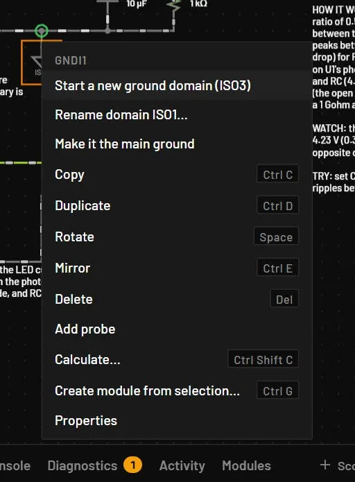
- To start a domain from a ground that's already placed, right-click it and choose Start a new ground domain (ISO3). That ground becomes the first symbol of the next free domain.
- To rename a domain, right-click any of its grounds and choose Rename domain ISO1…, type the new name and press Enter.You should seeEvery ground symbol, power flag, global label and net label of that name on the sheet takes the new name, in one undo step.
- To turn an isolated side back into the main ground, right-click one of its grounds and choose Make it the main ground.You should seeThe side joins net 0, and the ISO1 tied to GND tag and its warning go away. One undo brings the isolation back.
ResultEvery ground with the same name is one domain, with its own isolation resistance and capacitance. The inspector’s Ground name field does the same job by hand: empty, GND or 0 is the main ground, any other name is a domain.
| If you see | Do this |
|---|---|
| Pressing G again turned the ground instead of changing it | While placing, a part’s own key rotates it. Use Tab to change the domain. |
| The new name is refused | Names can't contain spaces, and GND and 0 mean the main ground: use Make it the main ground. |
See alsoKeep sides isolated with their own grounds, Labels, flags and ground.
10.5Select, move, copy and undo
Change the drawing without breaking connections.
- Click a part, or drag a box on empty canvas. Left to right selects what is fully inside, right to left also what it touches.
- Drag the selection to move it. Wires stretch to stay connected. The arrow keys nudge by one grid step, with Shift by five.
- Press Ctrl+D to duplicate, or Ctrl+C and Ctrl+V to paste at the pointer.You should seeCopies get the next free designators: R1 becomes R4 if R1 to R3 exist.
- Press Ctrl+Z to undo and Ctrl+Y to redo. Each tab keeps 300 steps.
ResultEvery edit, including a whole slider drag and an AI agent's edits, is one undo step.
10.6Find a part or a vendor model in the library
Find a part by its number, maker or function and place it with its model.
- Press / to jump to the library search.
- Type a part number, maker or function, for example
IRLZ44orlogic level mosfet. Every word must match. A value and a kind, such as10k resistor, offers a generic part with that value first.You should seeResults in sections: My parts, Symbols, Examples and Models. Exact part numbers come first, one row per part number with +N other models. - Optional: click a source chip such as TI or Verified only to narrow the list.
- Press Down to highlight a row and Enter to place it, or click a row, or drag it onto the canvas. Click the sheet to drop it.You should seeThe part is placed with its model, its pin map and its live values.
ResultSimulate runs the vendor's own file for that part. A green status dot means it runs in ngspice as it is.
| If you see | Do this |
|---|---|
| No results | The card shows near matches and Clear filters. Try a function search such as ldo 3.3. |
| A message that the model was replaced | The model fails in every engine. A working model of the same part was placed instead. |
10.7Type exact values and tune them with sliders
Set a part's value exactly, or sweep it by hand while the circuit runs.
- Click the part. The inspector shows its main parameters. Select several parts of one type to set them all at once.
- Click a field (its value is selected), type the value with an SI prefix, for example
4k7,100nor1Meg, and press Enter.You should seeThe value applies at once and keeps the circuit running. - To step to a neighbour, press Up or Down in the field, or PageUp and PageDown for the next standard value. The chevron at the right of the field lists the standard values.
- To tune, drag the slider under the field, or drag the field's label sideways. The whole drag is one undo step.
- Optional: set the slider's Min, Max and Log under it for a useful range. A field with no slider has a small slider button beside its label.
ResultThe value is saved with the part. Double-clicking a value label on the canvas edits it in place too.
| If you see | Do this |
|---|---|
| A red line under the field | The text isn't a value the part can take. 1,5 (comma decimal), 1.2.3, 12/3, junk after the number such as 4k7x, zero for a resistance and a negative delay are refused with a reason, and the old value stays. |
| A value a million times off | In fields, M is mega. Write 1Meg for mega and 1m for milli to be safe. |
See alsoTyping numbers, Sliders.
10.8Organise a big circuit with sheets and buses
Put a block of the circuit inside a box with ports, so the top sheet stays readable.
- Select the parts, wires and labels of the block.
- Press Ctrl+G. In the Create module dialog type a name, for example
HPF, check the pin names and directions, and press Enter.You should seeOne box replaces the selection, with a pin for every net that crossed its edge, inputs on the left and outputs on the right. Esc instead cancels and changes nothing. - Wire the box like a part, or join modules with net labels: a label on a pin, and the same label elsewhere on the sheet.
- Double-click the box to open it. Backspace with nothing selected goes back up. Double-click a pin to see its pin window (Alt+8).
- To add a pin later, use the pin window, or inside the module put a Sheet port (Alt+P) or a net label of the pin’s name on the net.
ResultThe circuit simulates exactly as before. Parts inside are named with a prefix, like S1/R3. Direction is only a label for drawing, sorting and monitoring.
See alsoHierarchical sheets and buses.
10.9Build the inside of a subcircuit myself
Place a box with pins and draw what is inside it, without a vendor model.
- Press X and place a Subcircuit / IC. Wire the circuit around it to its pins.
- Double-click it, or right-click it and choose Edit subcircuit.You should seeThe box becomes a sheet and opens in its own tab, ↳ X1, with one port for every pin.
- Draw the circuit between the ports, as on any sheet.
- Click the circuit's tab to go back to the top level, and ↳ X1 to go back in. The × on the ↳ tab closes only that tab.
ResultThe circuit runs with what you drew inside. One undo brings the plain box back.
| If you see | Do this |
|---|---|
| A double-click opens the model dialog | The part has a vendor model. Only a blank Subcircuit / IC can be edited this way. |
See alsoEditing a subcircuit.