
Devices: semiconductors
The diode, BJT, MOSFET (levels 1, 2 and 3, and VDMOS) and JFET use the same equations as ngspice, ported from its source: defaults, temperature scaling, junction limiting and convergence tests. A vendor .model card therefore gives the same result as in ngspice. Its parameters go on the part under their ngspice names in lower case.
32.1Where semiconductor values come from
| Source | What it sets |
|---|---|
| The inspector | The main parameters: is, n, rs, bv and cj0 for a diode, bf, is, vaf, cje and cjc for a BJT, vto, kp, lambda, cgs and cgd for a MOSFET. |
| A vendor model card | Assigning a model from the library merges every parameter of its card into the part. Simulate uses the vendor card itself. |
| Quick model | Datasheet values fitted exactly at the stated test point (Quick model tab). |
| A part file | Values from a .bspart. |
| The All parameters tab or the file | Any other ngspice parameter by its ngspice name. |
Shared instance parameters: temp (°C, default 27, the ngspice default), dtemp (offset from the circuit temperature), tnom (the temperature the model was measured at, default 27), mult (parallel devices), and area for diodes, BJTs and JFETs. Variants such as rectifier or darlington only change the symbol, except where the text says otherwise.
32.2Diode
| Type | Key | Pins | Variants | Class |
|---|---|---|---|---|
diode (D) | D | anode, cathode | rectifier, signal, schottky, zener, tvs, varactor, switching, fast (symbols). The bidirectional TVS is a separate model. | exact |
The ngspice junction diode: forward current IS (eV/(N·Vt) - 1), reverse breakdown at BV matched to IBV, series resistance, depletion and diffusion charge. A part placed from the library starts with is = 1 nA and n = 1.8.
| Parameter | Key | Unit | Default | Range | Value comes from | What it does |
|---|---|---|---|---|---|---|
| Saturation current | is | A | 10 fA | > 0 | Default, inspector, Quick model, board import, card | Alias js. |
| Emission coefficient | n | 1 | > 0 | Default, inspector, Quick model, card | ||
| Series resistance | rs | Ω | 0 | ≥ 0 | Default, inspector, Quick model, card | |
| Breakdown voltage | bv | V | none (no breakdown) | > 0 | Default, inspector, Quick model, card | A positive number. Aliases vb, vrb. |
| Breakdown current | ibv | A | 1 mA | > 0 | Inspector (Zener: Current at breakdown), Quick model (Zener), card | Current at bv. |
| Breakdown emission | nbv | = n | > 0 | Vendor model card, All parameters tab | ||
| Junction capacitance | cj0 | F | 0 | ≥ 0 | Default, inspector, Quick model, card | Zero-bias capacitance. Aliases cjo, cj. |
| Junction potential | vj | V | 1 | > 0 | Vendor model card, All parameters tab | Alias pb. |
| Grading coefficient | m | 0.5 | 0 to 0.999 | Vendor model card, All parameters tab | Alias mj. | |
| Forward-bias coefficient | fc | 0.5 | 0 to 0.999 | Vendor model card, All parameters tab | ||
| Transit time | tt | s | 0 | ≥ 0 | Quick model (t_rr / 1.5), card | Diffusion charge, sets reverse recovery. |
| Knee currents | ikf, ikr | A | none | > 0 | Vendor model card, All parameters tab | High-injection roll-off. |
| Recombination | isr, nr | A, - | none, 2 | ≥ 0, > 0 | Vendor model card, All parameters tab | |
| Sidewall | jsw, ns, cjp, php, mjsw, fcs, ikp | none, = n, 0, 1, 0.33, 0.5, none | Vendor model card, All parameters tab | Sidewall current and capacitance. | ||
| Tunnelling | jtun, jtunsw, ntun, xtitun, keg | none, none, 30, 3, 1 | Vendor model card, All parameters tab | |||
| Area, perimeter | area, pj | -, m | 1, 0 | > 0, ≥ 0 | Vendor model card, All parameters tab | |
| Temperature model | eg, xti, tlev, tlevc, cta, ctp, tpb, tphp, trs, trs2, tm1, tm2, ttt1, ttt2, tcv, gap1, gap2 | eg 1.11 eV, xti 3, others 0 | Vendor model card, All parameters tab | Temperature dependence of IS, BV, capacitances and resistances. |
Key: the name in the circuit file, in a parameter step (R1.r) and for AI agents. Range: a value outside it is refused with E_PARAM. Value comes from: where you can set it. The All parameters tab and agents can set every parameter.
Not implemented, so models that use them run approximately: LEVEL 3 geometry, RSW, soft recovery (VP) and self-heating. Typical values the inspector shows per variant: rectifier is 7 nA, n 1.98, rs 42 mΩ, bv 1000 V, cj0 26 pF. Signal: is 2.52 nA, n 1.752, bv 100 V, cj0 4 pF, tt 20 ns. Schottky: is 30 µA, n 1.05, bv 40 V, cj0 110 pF. Zener: bv 5.075 V, ibv 5 mA, rs 5 Ω. TVS: bv 6.7 V, cj0 1 nF. Varactor: bv 30 V, cj0 30 pF.
- Place a 12 V DC source, a 470 Ω resistor and a diode with its cathode towards the resistor and anode to ground.
- Select the diode, press Ctrl+Shift+M and type V_Z
3.3, I_Z20m, Z_Z10. Press Apply. - Hover the cathode wire.
You should seeThe cathode sits near 3.3 V. Change the source with its slider: the Zener voltage barely moves while the current through it changes.
32.3LED
| Type | Key | Pins | Variants | Class |
|---|---|---|---|---|
led (LED) | Shift+D | anode, cathode | standard, laser (symbols) | exact |
The diode model with colour-dependent defaults. It glows on the canvas in proportion to its current, full at 20 mA.
| Parameter | Key | Unit | Default | Range | Value comes from | What it does |
|---|---|---|---|---|---|---|
| Colour | color | red | red, orange, yellow, green, blue, white, uv, ir | Default, inspector | Sets is, n and rs unless they are given (is / n / rs): red 10-18 A / 1.9 / 2 Ω, orange and yellow 10-19 / 1.9 / 2, green 10-20 / 2.0 / 2, blue, white and uv 10-22 / 2.6 / 2, infrared 10-16 / 1.6 / 1. The inspector and All parameters show the values of the chosen colour, and the note under the colour gives the forward voltages. | |
| Saturation current | is | A | by colour | > 0 | Default, inspector, Quick model | |
| Emission coefficient | n | by colour | > 0 | Default, inspector, Quick model | ||
| Series resistance | rs | Ω | 2 | ≥ 0 | Default, inspector, Quick model |
Key: the name in the circuit file, in a parameter step (R1.r) and for AI agents. Range: a value outside it is refused with E_PARAM. Value comes from: where you can set it. The All parameters tab and agents can set every parameter.
32.4Bipolar transistor (NPN, PNP)
| Type | Key | Pins | Variants | Class |
|---|---|---|---|---|
npn, pnp (Q) | Q or Shift+Q | c, b, e | default, darlington (symbol), prebias (digital transistor with base resistors) | exact |
The ngspice Gummel-Poon model, with quasi-saturation (Kull) when rco is set. The prebias variant adds R1 in series with the base and R2 from base to emitter. The substrate capacitance goes to ground. A part placed from the library starts with bf = 100.
| Parameter | Key | Unit | Default | Range | Value comes from | What it does |
|---|---|---|---|---|---|---|
| Forward beta | bf | 100 | > 0. Slider 10 to 1000. | Default, inspector, Quick model, board import, card | Ideal maximum forward current gain. | |
| Saturation current | is | A | 10 fA | > 0 | Default, inspector, Quick model, card | |
| Early voltage | vaf | V | none (no Early effect) | ≥ 0 | Default, inspector, Quick model, card | Alias va. 0 also means none. |
| B-E capacitance | cje | F | 0 | ≥ 0 | Default, inspector, Quick model, card | With vje (0.75 V) and mje (0.33). |
| B-C capacitance | cjc | F | 0 | ≥ 0 | Default, inspector, Quick model, card | With vjc (0.75 V), mjc (0.33) and xcjc (1). |
| Forward emission | nf | 1 | > 0 | Vendor model card, All parameters tab | ||
| Knee current | ikf, nkf | A, - | none | ≥ 0 | Vendor model card, All parameters tab | Beta roll-off at high current. |
| B-E leakage | ise, ne | A, - | 0, 1.5 | ≥ 0, > 0 | Vendor model card, All parameters tab | Low-current beta. |
| Reverse | br, nr, var, ikr, isc, nc | 1, 1, none, none, 0, 2 | Vendor model card, All parameters tab | Reverse-active operation. | ||
| Resistances | rb, irb, rbm, re, rc | Ω, A | 0, 0, = rb, 0, 0 | ≥ 0 | Vendor model card, All parameters tab | Base resistance falls from rb to rbm with current. |
| Transit times | tf, xtf, vtf, itf, tr | s, -, V, A, s | 0, 0, none, 0, 0 | ≥ 0 | Vendor model card, All parameters tab | Diffusion charge, sets f_T and storage time. |
| Substrate | cjs, vjs, mjs, iss, ns, subs | 0, 0.75, 0, none, 1, ±1 | Vendor model card, All parameters tab | |||
| Quasi-saturation | rco, vo, gamma, qco, quasimod, vg, cn, d | off unless rco is set | Vendor model card, All parameters tab | Kull model with an extra collector node. | ||
| Prebias resistors | r1, r2 | Ω | 10 kΩ, 10 kΩ | > 0, ≥ 0 | Default, inspector | Prebias variant only. r2 = 0 removes R2. |
| Temperature model | eg, xti, xtb, tlev, tlevc and the t… coefficients | eg 1.11 eV, xti 3, others 0 | Vendor model card, All parameters tab |
Key: the name in the circuit file, in a parameter step (R1.r) and for AI agents. Range: a value outside it is refused with E_PARAM. Value comes from: where you can set it. The All parameters tab and agents can set every parameter.
Not implemented: excess phase (ptf) and self-heating. Typical values shown for a new NPN: is 6.7 fA, bf 200, vaf 74 V, cje 4.5 pF, cjc 3.6 pF. PNP: is 1.4 fA, bf 180, vaf 18.7 V.
32.5MOSFET (N, P)
| Type | Key | Pins | Variants | Class |
|---|---|---|---|---|
nmos, pmos (M) | M or Shift+M | d, g, s, and optionally b | enh, dep, 4pin, power, gan, sic | exact |
The ngspice MOSFET levels 1, 2 and 3, and the VDMOS model for power devices. With three pins the bulk is tied to the source. Variants that change the behaviour:
- dep: depletion mode, the threshold sign is flipped.
- power, gan, sic: a body diode from source to drain. A new part of these variants runs the VDMOS model with the values of a real part of its class (below), a part saved before with level 1 and bodyDiode on.
- 4pin: the symbol with the bulk pin.
- vdmos (from a vendor card or the file): the VDMOS model instead of level 1 to 3.
Where the engine deliberately differs from ngspice. A level 2 card with vmax (velocity saturation) and no nfs: between the flat-band voltage vbin and the threshold voltage ngspice solves a quartic for the saturation voltage whose root goes negative, and the channel then conducts a falling current although there is no inversion charge. A card with vto 0.72 V and gamma 0.94 V½ (vbin is then slightly below 0) conducts 47 µA at Vgs = 0 in ngspice. BetterSPICE holds the saturation voltage at zero there, so the device is off below its threshold, as the equations and the physics require (a CMOS output with its n-channel off reaches the supply rail: 5.000 V where ngspice shows 4.964 V). Above the threshold both give the same current to five digits. A level 2 part run in ngspice itself (a vendor-model Simulate, bspice ngspice) still shows ngspice's own sub-threshold current. The check is the known-difference entry of verification/circuits/semi/mos_cmos_l2_tran (PASS! in the verify list, Verification).
A plain MOSFET with no card uses level 1 with vto = ±2 V, kp = 0.1 A/V² and lambda = 0.01 /V. If rds_on is set and kp isn’t, kp = 1 / (rds_on · (10 - |vto|)), so rds_on is the on-resistance at 10 V of gate drive.
Default capacitances. Without gate capacitance a gate switches at once: no Miller plateau, no gate charge to drive. So a new generic MOSFET is placed with the capacitances of a real part of its class, taken from its datasheet and checked with a gate-charge test (constant gate current, clamped drain current, as the datasheets measure it). They are written into the part, so circuits saved before keep their results.
- enh, dep, 4pin N-channel (2N7000 class, 60 V 0.2 A): cgs 20 pF, cgd 6 pF. P-channel (BSS84 class, 50 V 0.13 A): cgs 50 pF, cgd 10 pF (Qgs 0.2 nC, Qgd 0.3 nC as the datasheet). The fixed cgd is the mean C_rss over the drain swing, so the gate charge is right although C_rss itself is larger at low voltage.
- power N-channel (IRLZ44N class, 55 V 47 A, logic level): VDMOS with vto 1.5 V, kp 20, rd 7 mΩ, rs 3 mΩ, rg 1.5 Ω, cgs 1.55 nF, cgdmin 40 pF, cgdmax 2.9 nF, a 0.4, cjo 1.4 nF, tt 8 ns. C_iss 1.70 nF, C_rss 151 pF, C_oss 397 pF at 25 V. Gate charge at 44 V, 25 A, 5 V: Qg 31.5, Qgs 4.8, Qgd 18 nC (datasheet maxima 48, 8.6, 25).
- power P-channel (IRF5305 class, -55 V -31 A): VDMOS with vto -3 V, kp 8, cgs 0.95 nF, cgdmax 2 nF, cjo 1.5 nF. Qg 42.7, Qgd 23.8 nC at -10 V (maxima 63, 29). The gan and sic symbols of a P-channel part get the same values (no such parts are made).
- gan (EPC2045 class, 100 V 16 A): VDMOS with vto 1.4 V, rg 0.6 Ω, cgs 0.76 nF, cgdmax 0.2 nF, cjo 0.8 nF, no body diode (it conducts backwards through the channel at about 1.6 V, as the datasheet’s 1.7 V). Qg 5.3, Qgs 1.8, Qgd 0.8 nC at 5 V (datasheet 6, 1.9, 0.8).
- sic (C3M0060065D class, 650 V 37 A): VDMOS with vto 2.3 V, rg 3 Ω, cgs 1.01 nF, cgdmin 6 pF, cgdmax 1.2 nF, cjo 0.6 nF, body diode about 5 V. C_rss 9 pF and C_oss 81 pF at 600 V. Qg 43.8 nC from 0 to 15 V at 400 V (datasheet 46 nC from -4 to 15 V).
The inspector shows one quiet line under the model of a generic MOSFET or IGBT: the class its capacitances are typical of. A larger part has more gate and output capacitance, and the package inductance (LG, LS, LD, a few nH each) is not in the part: draw it as inductors, or assign a vendor model, which has all of it. A part without any gate capacitance (one saved before) says so instead. The line is not shown for a part with a vendor model. No breakdown voltage is set, so a generic part used above its class does not clamp: set bv for avalanche. A part added with its own level-1 values (cgd, bodyDiode, rds_on or level) on a power symbol stays level 1, as does a vendor model’s fit.
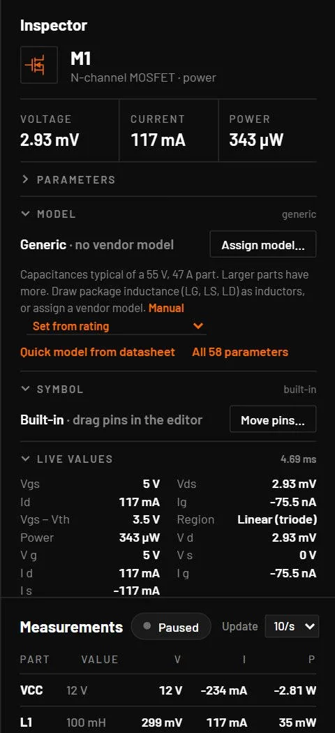
On an N-channel MOSFET the line ends in Set from rating, a menu of five classes, each with the values of one real part fitted to its datasheet: 30 V 5 A (AO3400A), 60 V 30 A (FQP30N06L), 100 V 50 A (IRF3710), 650 V SiC 30 A (C3M0060065D) and 100 V GaN 30 A (EPC2204). A choice fills the whole model as one undo step, switches the symbol to power, SiC or GaN as the part needs, and the line then names the part. The gate charge of each is within the datasheet’s typical or maximum values (docs/DEVICES.md lists them).
| Parameter | Key | Unit | Default | Range | Value comes from | What it does |
|---|---|---|---|---|---|---|
| Threshold | vto | V | 2 (pmos -2) | any. Slider -10 to 10 V. | Default, inspector, Quick model, board import, card | Alias vt0. |
| Transconductance | kp | A/V² | 0.1 | > 0 | Default, inspector, Quick model, card | |
| Channel-length modulation | lambda | 1/V | 0.01 | ≥ 0 | Default, inspector, Quick model, card | Output conductance in saturation. |
| Gate-source capacitance | cgs | F | 0 (placed with 20 pF, P 50 pF) | ≥ 0 | Default, inspector, Quick model | A fixed capacitor (BetterSPICE, not ngspice). Quick model: C_iss - C_rss. |
| Gate-drain capacitance | cgd | F | 0 (placed with 6 pF, P 10 pF) | ≥ 0 | Default, inspector, Quick model | A fixed capacitor. Quick model: C_rss. |
| On-resistance | rds_on | Ω | > 0 | Default, inspector | Sets kp as above. | |
| Body diode | bodyDiode | 0 / 1 | 1 for power, gan, sic | Default, inspector | IS 1 pA, N 1. | |
| Level | level | 1 | 1 to 3 | Vendor model card, All parameters tab | ||
| Bulk effect | gamma, phi | √V, V | 0, 0.6 | ≥ 0, > 0 | Vendor model card, All parameters tab | |
| Resistances | rd, rs, rsh, nrd, nrs | Ω | 0 | ≥ 0 | Vendor model card, All parameters tab | |
| Junctions | is, js, pb, cbd, cbs, cj, mj, cjsw, mjsw, fc | is 10 fA, pb 0.8 V, others 0 or 0.5 | Vendor model card, All parameters tab | |||
| Overlap capacitances | cgso, cgdo, cgbo | F/m | 0 | ≥ 0 | Vendor model card, All parameters tab | |
| Process | tox, uo, nsub, tpg, nss, ld, xj | tox none, uo 600 cm²/Vs | Vendor model card, All parameters tab | Derive vto, gamma, phi and kp when given. | ||
| Level 2 and 3 | delta, uexp, ucrit, vmax, neff, nfs, theta, eta, kappa, xl, wd, xw, delvto | ngspice defaults | Vendor model card, All parameters tab | |||
| Geometry | l, w, ad, as, pd, ps | m, m² | l = w = 100 µm | > 0 | Vendor model card, All parameters tab |
Key: the name in the circuit file, in a parameter step (R1.r) and for AI agents. Range: a value outside it is refused with E_PARAM. Value comes from: where you can set it. The All parameters tab and agents can set every parameter.
VDMOS cards add vto (default ±3 V), kp (20 or 10 A/V²), rd, rs, rg and rds. They also add quasi-saturation (rq, vq), the non-linear gate-drain capacitance (cgdmin, cgdmax, a), cgs, and a built-in body diode (is, n, rb, cjo, vj, m, tt, bv). Not implemented: self-heating and soft recovery. Typical values shown in empty fields of a new N-channel: vto 1.3 V, kp 0.2 A/V², cgs 20 pF, cgd 6 pF.
32.6JFET (N, P)
| Type | Key | Pins | Variants | Class |
|---|---|---|---|---|
njf, pjf (J) | J | d, g, s | none | exact |
The ngspice JFET with the Sydney University doping-tail parameter b. For a P-channel JFET, vto is entered as the P-channel value, positive for depletion.
| Parameter | Key | Unit | Default | Range | Value comes from | What it does |
|---|---|---|---|---|---|---|
| Pinch-off voltage | vto | V | -2 (pjf +2) | any | Default, inspector, Quick model, board import, card | Quick model: -|V_GS(off)|. |
| Transconductance | beta | A/V² | 1 mA/V² | > 0 | Default, inspector, Quick model, card | Quick model: I_DSS / vto². |
| Channel-length modulation | lambda | 1/V | 0 | ≥ 0 | Default, inspector, card | |
| Doping tail | b | 1 | Vendor model card, All parameters tab | |||
| Resistances | rd, rs | Ω | 0 | ≥ 0 | Vendor model card, All parameters tab | |
| Capacitances | cgs, cgd, pb, fc | F, V | 0, 0, 1, 0.5 | Vendor model card, All parameters tab | ||
| Gate junction | is, n | A, - | 10 fA, 1 | Vendor model card, All parameters tab | ||
| Temperature | tcv, vtotc, bex, betatce, xti, eg | 0, eg 1.11 | Vendor model card, All parameters tab |
Key: the name in the circuit file, in a parameter step (R1.r) and for AI agents. Range: a value outside it is refused with E_PARAM. Value comes from: where you can set it. The All parameters tab and agents can set every parameter.
32.7IGBT
| Type | Key | Pins | Variants | Class |
|---|---|---|---|---|
igbt (Q) | library | c, g, e | none | approximate |
A behavioural IGBT: an N-channel MOSFET behind a collector diode that gives the saturation knee. It has no reverse conduction: add an antiparallel diode for a co-pack.
| Parameter | Key | Unit | Default | Range | Value comes from | What it does |
|---|---|---|---|---|---|---|
| Threshold | vth | V | 5 | any. Slider 1 to 10 V. | Default, inspector | |
| Transconductance | kp | A/V² | 1 | > 0 | Default, inspector | |
| V_CE(sat) | vce_sat | V | 1.5 | ≥ 0 | Default, inspector | On-state voltage scale at about 1 A. |
| Gate capacitances | cgs, cgd | F | 0 (placed with 0.9 nF, 0.2 nF) | ≥ 0 | File or All parameters only | A new IGBT gets the values of a 600 V, 20 A part (IKW20N60T: C_ies 1.1 nF, Q_G 120 nC at 480 V). cgd is the mean C_res over the collector swing, so the gate charge is right (112 nC). Package inductance is drawn as inductors. |
Key: the name in the circuit file, in a parameter step (R1.r) and for AI agents. Range: a value outside it is refused with E_PARAM. Value comes from: where you can set it. The All parameters tab and agents can set every parameter.